
Siemens has acquired Canopus AI, adding computational metrology and inspection software to its electronic design automation portfolio as chipmakers seek tighter process control in advanced manufacturing.
Canopus AI develops AI-driven metrology and inspection technology used in wafer and mask manufacturing. Siemens said the deal broadens its semiconductor design-and-manufacturing "digital thread" by linking metrology data more directly to design and process engineering workflows.
Founded in 2021, Canopus AI is based in Grenoble, France. The company focuses on software for measurement and inspection steps that sit alongside lithography, process simulation and manufacturing execution in a semiconductor fab.
Metrology focus
Metrology and inspection have become more central to semiconductor production as device geometries shrink and manufacturers scale output. Smaller features require tighter monitoring of pattern fidelity across wafers and masks. Inspection systems also generate large volumes of data that engineers use to diagnose process drift and identify yield issues.
Siemens plans to integrate Canopus AI's software with its Calibre product line, widely used for physical verification and sign-off in chip design. The combination is intended to link manufacturing-physics simulation with measurement and inspection analysis, creating what Siemens described as an end-to-end EDA digital thread spanning design through manufacturing.
"The acquisition of Canopus AI exemplifies Siemens' commitment to leveraging industrial AI to solve critical challenges in semiconductor manufacturing," said Tony Hemmelgarn, President and CEO, Siemens Digital Industry Software.
"By combining the computational lithography and manufacturing physics simulation capability in our Calibre portfolio with Canopus-AI's advanced metrology and inspection technologies, we are creating a differentiated, end-to-end EDA digital thread that improves the fidelity of printed wafer patterns, accelerates yield ramp and reduces time-to-volume for advanced nodes. This integration further advances our vision of a comprehensive, high-accuracy, semiconductor manufacturing digital twin, enabling sub-nanometer process control and mask development."
Software elements
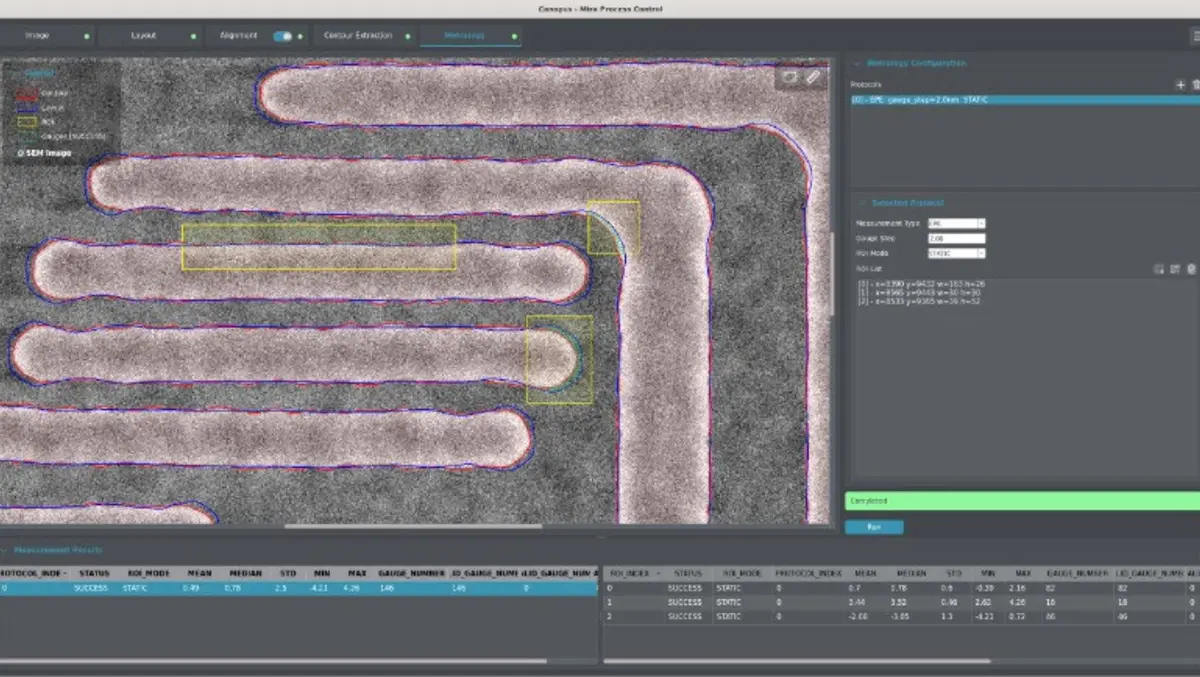
Canopus AI's technology includes machine learning methods that analyse metrology and inspection results. One use is measuring edge placement error, a metric that compares intended and printed patterns. The output can feed back into wafer-manufacturing simulation models.
The company also offers a web-based viewer for critical-dimension scanning electron microscope images and high-volume manufacturing data review. It uses a map-style interface to navigate large image sets and associated measurement information.
Another element is data handling that spans pixel-based image data and vertex-based representations. Canopus AI also supports native multigon curvilinear data, used when designs include more complex geometries than traditional rectilinear shapes.
Industry context
Large chipmakers and foundries have increased spending on process control as they adopt new materials and patterning techniques. Inspection and metrology have expanded beyond sampling to more frequent measurement, including steps that attempt to correlate in-line and end-of-line results. The goal is to detect defects earlier and more tightly control critical dimensions.
In that environment, software that connects design intent, lithography settings, process models and measured outcomes has become more important. EDA suppliers have also tried to deepen their presence in manufacturing by linking verification tools with fab data and expanding into areas such as computational lithography and advanced process control.
Siemens has positioned its semiconductor software business around tighter links between design and manufacturing, with Calibre as the cornerstone for physical verification. The Canopus AI acquisition adds inspection and metrology analytics closer to the production line, potentially widening Siemens' role in yield engineering and process-monitoring workflows.
Customer reach
Canopus AI said joining Siemens will expand its reach across the EDA user base and semiconductor manufacturing customers. "We are delighted to join Siemens and bring the power of AI-enabled metrology in the semiconductor industry to a broader audience as part of Siemens' EDA community of users," said Joël Alanis, Chief Executive Officer of Canopus AI.
"Together, we'll empower innovators pushing the boundaries of semiconductor design and manufacturing with robust wafer and mask metrology and inspection and help them to meet the challenges of the rapidly changing semiconductor industry," Alanis said.